-
E-mail
kunhoujc@163.com
-
Phone
18126732791
-
Address
10-1307, Hejin Industrial Park, No. 895 Asian Games Avenue, Panyu District, Guangzhou City
Product Categories
Guangzhou Kunhou Testing Technology Co., Ltd
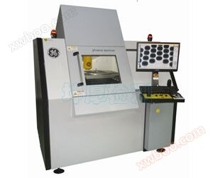
Phoenix X | Aminer entry-level X-ray detection system
NegotiableUpdate on 03/17
- Model
- Nature of the Manufacturer
- Producers
- Product Category
- Place of Origin
Overview
Phoenixx | Aminer is an easy-to-use entry-level X-ray testing system with high-performance microfocus non-destructive testing equipment. It is designed specifically for high-resolution testing requirements in fields such as semiconductor packaging, electronic components, and electronic assembly
Product Details
Phoenix X | Aminer is an easy-to-use entry-level X-ray testing system with high-performance microfocus non-destructive testing equipment. It is designed specifically for high-resolution testing requirements in fields such as semiconductor packaging, electronic components, and electronic assembly We are now equipped with a new type of CMOS flat panel detector, which has better signal-to-noise ratio, clarity, and real-time imaging capability than image intensifiers, and can also choose CT function The system provides powerful and user-friendly Phoenix X | ACT Base 2D software and Datos | X Base CT software, and allows manual detection and programmed automatic detection
Main features and benefits
160kV/20W high-power X-ray tube with no service life limit, easy to penetrate high absorbing workpieces
Optional high contrast CMOS flat panel detector with better real-time detection capability
Comprehensive CT software module with simple and fast operation
Humanized design and easy-to-use operation
Real time CAD data matching capability
Automatic real-time navigation map function, easy to quickly locate the upper and lower surfaces and interior of the sample
Laser anti-collision design to protect workpieces
compact footprint
Installed printed circuit board2D X-ray image of µ BGA
Power electronic devicesSolder the surface of power semiconductor components onto a ceramic substrate. After passing through a 3mm thick copper heat sink, voids can be seen on the substrate, and there are no voids in the semiconductor solder joints. Even thin aluminum solder wires can be seen.
|
Semiconductors and other electronic componentsReal time images can be obtained by matching real-time CAD data from any detection angle at any time.
CT image
|
Similar Product Recommend