-
E-mail
kunhoujc@163.com
-
Phone
18126732791
-
Address
10-1307, Hejin Industrial Park, No. 895 Asian Games Avenue, Panyu District, Guangzhou City
Product Categories
Guangzhou Kunhou Testing Technology Co., Ltd
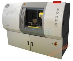
Phoenix Nanotom m CT Detection System
NegotiableUpdate on 03/17
- Model
- Nature of the Manufacturer
- Producers
- Product Category
- Place of Origin
Overview
phoenixnanotom ® M is a nanoCT ® The system is used for scientific and industrial computed tomography (microct and nanoct) and three-dimensional measurement of a wide range of samples
Product Details
phoenix nanotom ® M is a nanoCT®The system is used for scientific and industrial computed tomography (micro CT and nano CT) and three-dimensional measurement of a wide range of samples. With its specially designed 180 kV/15 watt high-power nanofocus X-ray tube with internal cooling and temperature stable digital detector, the system achieves unique spatial and comparative resolution for a wide range of samples and applications - from small biological and geological specimens to medium-sized industrial components such as injection ports or injection molded plastic parts - as well as metal inlays. The fully automated execution, reproduction, and analysis process of CT scanning ensures its usability as well as fast and reliable CT results. Once scanned, full 3D CT information can provide many possibilities for analysis, such as non-destructive visualization of slices, arbitrary cross-sectional views, or automatic pore analysis. It is possible to scan the entire geometric shape of an object, perform precise and reproducible 3D measurements of complex objects, and automatically generate first article inspection records within one hour.
Features:
Main functions
The extremely high image quality of the unique temperature stable digital GE DXR detector (3072 x 2400 pixels) is used for high dynamic range>10000:1
The new open 180 kV/15 watt high-power nanofocus X-ray tube has a detail detection capability of up to 200 nanometers and internal cooling - the best for long-term stability
-
The measurement beam used for 3D measurement applications includes:
Temperature stable cabinet
High precision direct measurement system
Vibration prevention of the manipulator
Diamond | Window
2 calibration targets
Phoenix datos | x 2.0 software package "Click&Measure CT" and 3D "Measurement“
Customer benefits:
Unique spatial and comparative resolution across a wide sample range - from small materials to medium-sized plastic samples containing three orders of magnitude (0.25mm to 250mm sample size and 3kg/6.6lb sample weight),
The best 3D measurement package is used for stable acquisition conditions, fast reconstruction within minutes, and reproducible measurement results
The best usability comes from system design and advanced Phoenix Datos | x 2.0 CT software
Diamond shaped windows can achieve extremely high focal stability and perform data acquisition up to twice as fast with the same level of high image quality
Application:
3D computed tomographyThe classic application of industrial X-ray 3D computed tomography (micro CT and nano CT) is the detection and 3D measurement of metal and plastic castings. However, the high-resolution X-ray technology of Phoenix has opened up new applications in many fields, such as sensor technology, electronics, materials science, and many other natural sciences. NanoCT for SMD sensors ®, Size 0805 (2.0mm x 1.2mm) The 3D X-ray image shows the internal coils behind the back cover. In any conventional X-ray, the layer panels overlap, but nanoCT ® Successfully displayed objects layer by layer. Materials ScienceHigh resolution computed tomography (micro CT and nano CT) is used for detecting materials, composite materials, sintered materials, and ceramics, but it is also used for analyzing geological or biological samples. The material distribution, porosity, and cracks are visible in three dimensions at a microscopic resolution. NanoCT of glass fiber composite materials ®: The fiber direction of the fiber felt (blue) and the matrix resin (orange) will be displayed. On the right: The voids inside the resin will appear as dark cavities. Left: The resin has gradually disappeared to better visualize the fiber felt. The single fiber inside the felt is visible. Sensors and Electrical EngineeringIn the detection of sensors and electronic components, high-resolution X-ray technology is mainly used to detect and evaluate contact points, joints, boxes, insulators, and assembly conditions. It can even detect semiconductor components and electronic devices (solder joints) without disassembling the equipment. nanoCT ® Display the welding joints of CSP components. The three-dimensional shape of the welded joint is approximately 400 microns in diameter, with clear and visible gap distribution. Inside the welding joint, different eutectic solder phases are visible. |
measurementThe three-dimensional measurement using X-rays is the only technique that can perform non-destructive measurements on the interior of complex objects. By comparing with traditional tactile coordinate measurement techniques, computerized tomography of an object can simultaneously obtain all surface points - including all concealed forms that cannot be accessed without damage using other measurement methods, such as bottom cuts. V | tom | x s has a special 3D measurement package that includes all the tools needed for spatial measurement, from calibration instruments to surface extraction modules, with the highest possible accuracy, reproducibility, and ease of use In addition to two-dimensional wall thickness measurement, CT volume data can be quickly and conveniently compared with CAD data, for example, to analyze completed components to ensure they meet all specified dimensions. CAD difference analysis and measurement of three cylinder head devices. Plastic EngineeringIn plastic engineering, high-resolution X-ray technology is used to optimize casting and spraying processes by detecting shrinkage cavities, bubbles, welding lines, and cracks and analyzing vulnerabilities. X-ray computed tomography (micro CT and nano CT) provides three-dimensional images of objects with characteristics such as grain flow patterns and filler distribution, as well as low contrast defects. Glass fiber increase?? NanoCT of Strong Plastic Samples ®: The arrangement and distribution of aggregates of glass fibers and mineral fillers (purple) are clearly visible. The fibers are approximately 10 microns wide. Geological/Biological SciencesHigh resolution computed tomography (micro CT and nano CT) is widely used for detecting geological samples, such as exploring new resources. The high-resolution CT system provides three-dimensional images of rock samples, binders, adhesives, and voids at microscopic resolution, and helps confirm specific sample features such as the size and location of voids in oil bearing rocks Segmented pores in carbonates (ø 2mm) |
Specifications:
| Maximum tube voltage | 180 kV |
|---|---|
| maximum power | 15 watts |
| Detail detection capability | Up to 200nm (0.2 µ m) |
| Focal distance measurement | 150mm to 600mm |
| Minimum voxel size | < 300nm (0.3µm) |
| Geometric magnification (3D) | 1.5 times to 300 times |
| Maximum target size (height x diameter) | 250mm x 240mm/9.84 "x 9.45" |
| Maximum object weight | 3 kg/6.6 pounds |
| Image Chain | 7-megapixel flat panel digital detector array |
| 2D X-ray imaging | No |
| 3D computed tomography | can |
| Advanced surface extraction | Sure (optional) |
| CAD comparison+dimension measurement | Sure (optional) |
| System size | (1980 x 1600 x 900 millimeters), (78 "x 63" x 35.4 ") |
| System Weight | 1900 kg/4189 pounds |
| Radiation safety | -Fully radiation resistant safety cabinet, in accordance with German ROV (Attachment 2 nr. 3) and American performance standard 21 CFR 1020.40 (Cabinet X-ray System) -Emission limit for exposure<1 µ Sv/h, measured from a distance of 10 centimeters from an accessible surface |
Similar Product Recommend